Research
Our group employs density functional theory in order to understand material properties and think industrial applications from computational results.
1. Materials for next-generation power electronics: SiC and GaN
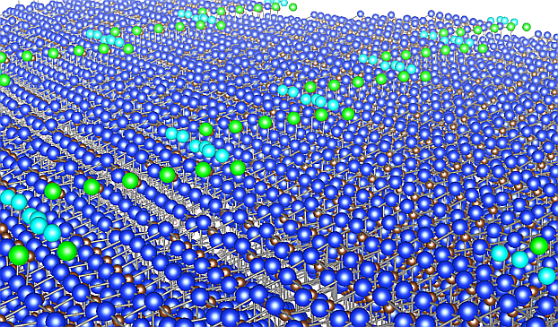
Figure 1: Meandering step structures on the vicinal SiC surface[K.Seino and A. Oshiyama, Appl. Phys. Exp. 13, 015506 (2020).]
Wide bandgap semiconductors are attractive candidates for next-generation high-power devices and can replace current Si technology for power electronics. Two promising materials for this purpose are SiC and GaN. SiC metal-oxide-semiconductor field-effect transistors (MOSFETs) are already on the market. Favorable transport properties of GaN are suitable for high-power and high-frequency electronics. Therefore, the development of both SiC- and GaN-power electronics technologies is expected.
For SiC, we investigated SiC stepped surfaces. The surface steps also provide stages for materials syntheses. Yet to unveil the underlying rationale behind the phenomena related to the atomic steps on the surface, the identification of abundant step structures and the clarification of the energetics of various atomic steps are indispensable and highly demanded in both science and technology. Hexagonal SiC(0001) and cubic SiC(111) surfaces, that are the Si-face SiC polar surfaces, are commonly used for the SiC epitaxial growth. It is known that there are variations of the step morphology depending on the inclined direction. We performed large-scale density-functional calculations using the real-space finite-difference scheme that reveal detailed atomic and electronic structures of atomic steps on SiC surfaces(Figure 1).
For GaN, we are now investigating defects in GaN, in particular, acceptor impurity in p-GaN. One of the key technologies for high-performance GaN power devices is selective doping for p-type GaN using ion implantation. However, the activation of implanted Mg ion is an unresolved issue in this technique. Theoretical approaches can be valuable to clarify physics and diffusion mechanisms for defect systems in semiconductors.
2. Si nanostructures for application to Si-based solar cells
One way to improve Si-based photovoltaic solar energy performance is to absorb photons by processes involving multiple energy thresholds, such as in multiple quantum wells (MQWs), e.g., occurring in tandem cells. There are theoretical predictions that the cell efficiency can be improved towards 66 % using an optimum band structure design of Si/SiO2 layered systems. In the case of Si-based solar cells, the only way for a gap variation is nanostructuring, leading to a gap widening by quantum-size effects.
We focused on Si/SiO2 MQWs and Si nanocrystals (Si NCs) embedded in SiO2 as Si nanostructures for Si-based solar cells. Properties of Si NCs shown in Fig. 2 have been experimentally and theoretically widely studied due to their efficient light emission with foreseen application. The Si NC properties appear to be very sensitive to their Si/SiO2 interface and their size distribution. In this study we present theoretical investigation of Si NCs with different sizes embedded in an amorphous SiO2 matrix based on density-functional theory. In our simulations realistic Si nanocrystals with diameters ranging between 0.8 and 1.6 nm, i.e., up to systems with more than 1000 atoms, are treated. The atomic geometries are optimized within quantummechanical calculations. We also compare with hydrogenated Si NCs of corresponding size and shape. We demonstrate the influence of the interface between NC and matrix on the electronic and optical properties (Figure 3). Moreover, we compute the spatial variation of the electronic structure for embedded Si NCs as an example for interfacial electronic properties of non-planar interfaces.
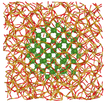
Figure 2: Model of a Si nanocrystal (NC) embedded in SiO2 with a diameter of 1.6 nm[K.Seino et al., Nanotechnology 20, 135702 (2009).]
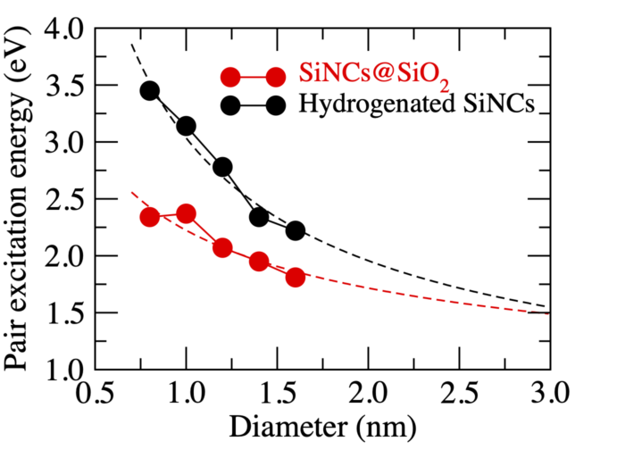
Figure 3: Pair excitation energies versus NC diameter for Si NCs embedded in amorphous SiO2 and hydrogenated Si NCs.
3. One-dimensional metallic nanowire on semiconductor surfaces
Figure 4: Wave-function square of a surface band of Si(111)-(5×2)-Au surface[K.Seino and F.Bechstedt, Phys. Rev. B 90, 165407 (2014).]
One-dimensional (1D) electronic systems have been investigated extensively because of the interest both in fundamental physics and in nano or atomic scale devices. Self-assembled atomic scale nanowires provide ideal systems for studying peculiar properties of 1D electronic systems. Metallic atomic wires, consisting of self-organized atomic chains of Au, Pt, In or Pb grown on Si or Ge surfaces, are prototype of such a 1D systems. Density-functional theory (DFT) calculations were decisive for determining the geometry of many 1D and quasi-1D structures. They helped, in particular, to identify atomic configurations and chemical trends.
We considered two types of Au-induced wire structures on Si or Ge semiconductor surfaces. The first system consists of Si(111)-(5×2)-Au wires shown in Fig. 4, while the other system are Au-induced nanowires on the Ge(001) substrate.
4. Functionalization of Si(001) surface by organic molecules
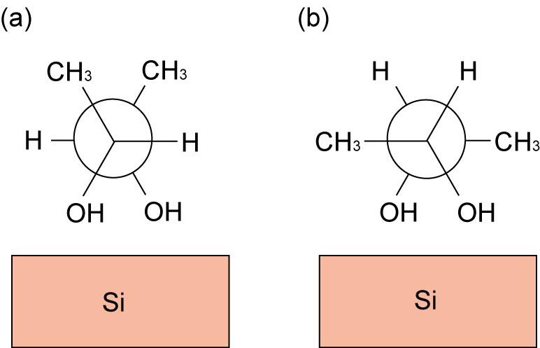
Figure 5: Schematic illustration of (R,R)-2,3-butanediol adsorption on Si(001) for different confirmation.[K.Seino and W.G.Schmidt, Surf. Sci. 585, 191 (2005).]
Fundamental and technological interest in organic adsorption on Si surfaces is due to the vast range of qualities that organic molecules can be designed to have, and the hope of adding their functionality to semiconductor technology. Particularly interesting are surface reactions with polyfunctional organic molecules. They may allow for creating an ordered array of possible reaction sites, provided the functional groups remain intact. It is possible to form well-ordered organic layers on Si(001) surfaces using the cycloaddition reaction between Si surface dimers and carbon double bonds in unsaturated organic molecules.
We perform density-functional calculations that unveil structural and electronic properties and reaction process on various organic molecules on Si(001) surfaces. Figure 5 is an example, (R,R)-2,3-butanediol adsorption on Si(001) for different confirmation. We analyzed computational reflectance anisotropy spectroscopy (RAS) spectra for these systems and shown different peak positions. Our results will provide guidance for experiments.
Knowledge for clean surfaces is also important. The atomic configuration of the Si(001) surface at very low temperatures has again become once controversial. In elucidating the mechanism of the structural phase transition between the c(4×2) and p(2×2) reconstructions, we pointed out the effects of external electric fields and the injection of electrons and holes into surfaces.
5. Atomic structures of GaAs(001) surface and its microscopic epitaxial growth process
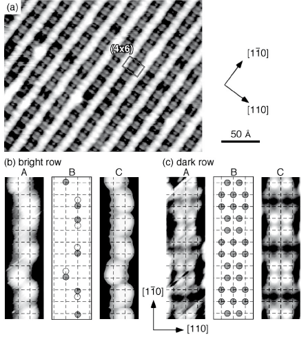
Figure 6: Typical filled-state STM images obtained from the GaAs(001)-(4×6) surface with atomic positions of surface atoms (parts B) and simulated STM images (parts C).[A.Ohtake et al., Phys. Rev. Lett. 93, 266101 (2004).]
The GaAs(001) surface belongs to the most intensively investigated compound semiconductor surfaces shows a variety of reconstructions depending on surface stoichiometries. A series of Ga-rich GaAs(001)-(4×6) and -(6×6) reconstructions, which have a larger periodicity than (4×2) reconstructions, also have been reported from scanning tunneling microscope (STM) observations. Therefore, the information from computational works was expected to understand detailed atomic structure. We performed total-energy calculations that clarify atomic structures for Ga-rich GaAs(001)-(4×6) and - (6×6) reconstructions and obtained theoretical STM images (Figure 6).
Moreover, in the atomic-level control of semiconductor epitaxial growth, it is important to clarify the microscopic motion of atoms, the so-called diffusion mechanism. We have also clarified the adsorption and diffusion mechanisms of surface atoms for several reconstructed structures on Ga-terminated surfaces, thereby providing insight into the atomic-level dynamic processes on both As- and Ga-terminated surfaces, and deepening our understanding of the fundamental mechanisms underlying semiconductor epitaxial growth.
